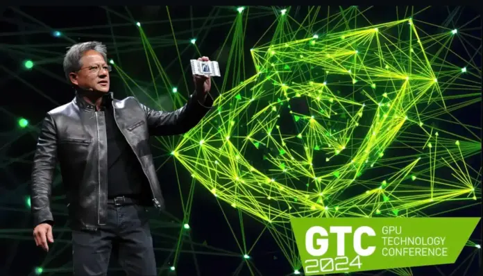
As expected, Nvidia presented the new Blackwell architecture at GTC 2024. With the B200 chip and the GB200 platform, the manufacturer is entering new spheres
As expected, Nvidia presented the new Blackwell architecture at the ongoing GTC 2024 (GPU Technology Conference) on Monday night, promising to set new standards.
As Nvidia CEO Jensen Huang fittingly explained, this is intended to usher in a “new era of generative AI”. At the spearhead of this is the B200 chip, which replaces the previous H100 and GH100 flagships from the Hopper generation
The impressive technical specifications (see below) suggest that major customers such as Amazon and Microsoft with the corresponding demand and budget will be queuing up at Nvidia to get as many of these chips as possible.
The most important things in a nutshell
- Nvidia presents the new Blackwell architecture for generative AI at GTC 2024.
- The B200 chip replaces the H100 and GH100 flagships and offers improved performance and energy efficiency.
- The GPU is based on a 4nm manufacturing process and has 208 billion transistors.
- The GB200 superchip combines Grace processors, Blackwell GPUs and offers extremely high computing power.
Technical data of the Nvidia B200
The GPU is developed on the basis of the 4NP production process – a special 4 nm production process designed for Blackwell by the Taiwanese chip manufacturer TSMC.
The B200 itself is a dual-die design. The two built-in chips communicate via a slide-to-die link at a speed of up to 10 TByte per second and should therefore have no disadvantages compared to the MCM (Multi Chip Module) process, which is primarily used by AMD.
There are a total of 208 billion transistors in the B200 card. According to Nvidia, the theoretical computing power is as follows:
- FP8: Up to 20 PetaFLOPS
- FP16: Up to 10 PetaFLOPS
- FP32: Up to 5 PetaFLOPS
According to Huang, this should result in around four times the performance for AI training and 30 times the performance for AI inference. Meanwhile, energy efficiency is to be improved by a factor of 25.
On the memory side, Nvidia B200 works with 192 GByte HBM3e memory, the bandwidth should be up to 8 TByte/s.
“Grace Blackwell” as a new superchip
The new chip also forms the basis for the “Grace Blackwell” superchip called GB200, which will primarily be used in Nvidia’s own NVL72 computer and customer-specific solutions.
True to its name, the GB200 Grace Blackwell is a hybrid solution consisting of a Grace processor with 72 Neoverse V2 cores from the manufacturer Arm and two of the B200 graphics chips shown – so a single GB200 chip has four dies in this respect.
In the NVL72 computer mentioned above, 36 of the Grace CPUs are used together with 72 Blackwell GPUs (and consequently 144 Blackwell dies), which results in the following insane technical data:
- Processor: 2,592 ARM Neoverse V2 cores
- Memory: Up to 17 TByte LPDDR5X RAM
- 72 Blackwell GPUs with 13.5 TByte HBM3e memory
- FP4 computing power: Up to 1,440 PetaFLOPS
- FP8 computing power: Up to 720 PetaFLOPS
- FP16 computing power: Up to 360 PetaFLOPS
Thanks to NVLink, which promises up to 130 TByte per second of bandwidth, the NVL72 supercomputer should behave like a single massive graphics processor
A total of up to 576 GPUs can be connected in such an NVLink domain – according to Huang, the total computing power should be sufficient to process Large Language Models (LLMs) with trillions of parameters.
The assumed power consumption is correspondingly high: a single GB200 superchip is said to require up to 2,700 watts.
The first business customers are already queuing up The AI platform should be available for business partners in the course of the year. Nvidia explicitly mentions cloud providers such as AWS, Google Cloud, Microsoft Azure and Oracle Cloud Infrastructure, which are unsurprisingly showing interest in the Blackwell architecture. As Huang explains, Nvidia is on the verge of the “most successful launch in the company’s history” with Blackwell.


